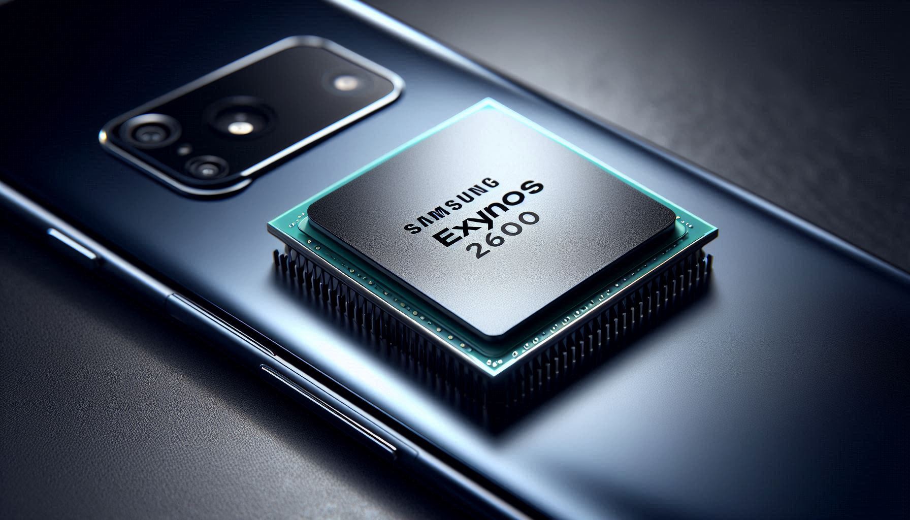
Samsung has officially introduced the Exynos 2600, the world’s first smartphone processor built using an advanced 2-nanometer (2nm) Gate-All-Around (GAA) process, marking a major milestone in mobile chipset technology. This next-generation System-on-Chip (SoC) is expected to power flagship devices like the Galaxy S26 series in many regions and bring improvements in performance, AI capabilities, graphics, and energy efficiency.
A Leap Forward in Chip Technology
The Exynos 2600 stands out as the first mobile SoC manufactured on the 2nm GAA node, a process that enhances transistor control, boosts energy efficiency, and delivers higher sustained performance compared with 3nm chips. This gives Samsung an early edge over rivals, as Qualcomm and other manufacturers are still on earlier process nodes.
Performance and Architecture
Samsung has redesigned the processor’s internal structure with a 10-core CPU based on Arm’s latest architecture, including:
One high-performance C1-Ultra core up to 3.8GHz
Three high-performance C1-Pro cores at 3.25GHz
Six additional C1-Pro cores tuned for sustained efficiency
This architecture delivers up to 39 percent improved CPU performance compared with its predecessor, the Exynos 2500, while also improving power efficiency for longer battery life.
Graphics and AI Upgrades
The Exynos 2600 integrates a Samsung Xclipse 960 GPU, which reportedly offers up to twice the graphics performance and 50 percent better ray tracing than the previous generation. This GPU also includes AI-based upscaling and frame generation for smoother gaming on high-resolution displays.
AI performance is dramatically boosted thanks to a powerful Neural Processing Unit (NPU) designed for on-device generative AI and machine learning tasks. Samsung claims the NPU delivers over 100 percent faster AI performance, enabling smarter photo processing, voice recognition, and other AI-driven experiences without relying on cloud services.
Camera and Multimedia Capabilities
The Exynos 2600 supports advanced imaging features, including:
Up to 320MP single-camera sensors
Zero shutter lag for 108MP photos
8K video recording at 30fps and 4K at 120fps with HDR
Advanced video noise reduction and AI-assisted visual enhancements
These improvements position the chip for premium photography and creative workflows directly on the device.
Better Efficiency and Thermal Control
To address thermal challenges common in high-performance chips, Samsung has integrated a Heat Path Block (HPB) thermal solution, using advanced materials to improve heat dissipation and lower thermal resistance by up to 16 percent. This is designed to help the chipset maintain stable performance during intense tasks like gaming and AI computations.